
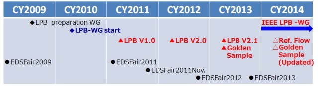
Established preparation Working Group in July 2009、Formally inaugurated in April, 2010
Activity record JEITA LPB interoperable design process WG (shown above)
-In the panel discussion in January 2009 EDS Fair 2009, Discussed the issues in the overall design
of the LPB, and concluded the need for coordination in LPB design parties.
-July 2009, Established as a preparation WG.
-April 2010, Started as official WG.
-January 2011, In the panel discussion EDS Fair 2010, discussed the need for common standards
in the LPB.
-March 2011, LPB V1.0 ; Developed first common standards.
-November 2011, EDS Fair 2011 November, Introduced an example design using a common standard.
-March 2012, EDA vendor seminar
-March 2012, LPB Ver. 2.0 ; formal production version.
-November 2012, Exhibition in EDSFair2011 / Panel discussion in SDF2011: discuss about 'Value chain'
-March 2013, Establishe LPB forum, 1st LPB Forum
-March 2013, LPB Ver.2.1 ; updated
-June 2013, Exhibition in DAC2013
-September 2013, 2nd LPB Forum; Reference flow workshop
-November 2013, Exhibition in EDSFair2013 / Panel discussion in SDF2013(3rd LPB forum): real case study of reference flow
Configuration of committee
2010, 16 companies, 20 formal members, 3 special members, 1 academic member.
2011, 16 companies, 22 formal members, 2 special members, 1 academic member.
2012, 17 companies, 21 formal members, 4 special members, 1 academic member.
2012, 13 companies, 20 formal members.
Committee consists of diverse parties; semiconductor, set , EDA, University.
■inquiry to JEITA EDA Technical Committee
■inquiry to LPB Semiconductor & System Design Technical Committee